| improving performance |
|
Great strides have been made in recent years in enhancing the performance of CCDs. In this section, we shall briefly look at how four of the most important characteristics of CCDs can be improved: dark current, quantum efficiency, readout speed and readout noise.
dark current
Valence electrons in a CCD can be promoted into the conduction band by absorbing energy, either from the random thermal (i.e. heat-generated) motion of the atoms in the silicon lattice, or from an incoming photon. The former mechanism is known as dark current and the electrons produced by it are indistinguishable from photo-electrons.
Dark current can be very substantial. At room temperature, the dark current of a standard CCD is typically 100,000 e-/pixel/s, which is sufficient to saturate most CCDs in only a few seconds. One way round this is to take very short exposures, but astronomical sources are usually too faint for this to be possible without paying a heavy penalty in readout noise.
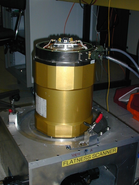
The solution is straightforward - cool the CCD. Dark current decreases rapidly with decreasing temperature. The typical operating temperatures of CCDs are in the range 150 to 263 K (i.e. -123 to -10oC). At major observatories, most CCDs are cooled to the bottom end of this range, generally using liquid nitrogen. The resulting dark current can be as low as a few electrons per pixel per hour. To prevent the liquid nitrogen from having to be continuously replenished as it boils off, CCDs are usually mounted in cryostats, as shown in figure 111. Cryostats employ a vacuum and radiation shield to minimize conductive and radiative heating by the surroundings.
| figure 111: |
Photograph of the gold-coloured ULTRASPEC cryostat in the lab, with the lid open. The CCD mounted on its circuit board can be seen at the top.
|
quantum efficiency
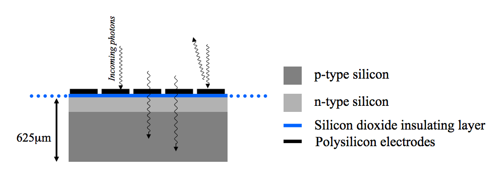
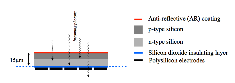
Thus far, we have been considering CCD structures which involve the photon passing through the electrode structure to get to the depletion region in the silicon substrate beneath. Unfortunately, the electrode structure absorbs and reflects many of the incident photons, particularly at blue wavelengths, preventing them from producing electron-hole pairs in the depletion region. This arrangement is known as a front-side illuminated CCD, and is illustrated in the top panel of figure 112.
| figure 112: |
Top: schematic of a thick, front-side
illuminated CCD. Bottom: schematic of a thinned, back-side
illuminated CCD.
|
The percentage of photons incident on a CCD which successfully produce electrons that are measured at the output of the CCD is known as the quantum efficiency (QE) of the device. The QE varies with wavelength and, for a front-side illuminated device peaks around 50%, as shown in figure 113. As well as absorbing photons, the complicated nature of the electrode structure precludes the use of an anti-reflection (AR) coating, which would otherwise boost the QE of a front-side illuminated CCD.
| figure 113: |
Graph comparing the QE of a thick
front-side illuminated CCD with that of a thinned, back-side illuminated CCD.
|
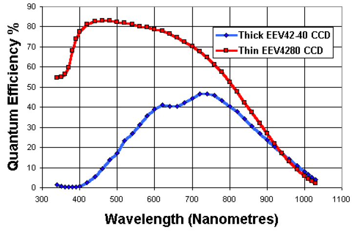
One way to significantly improve the QE of a CCD is to turn it over and illuminate it from the back side. The photons in such a back-side illuminated device do not have to pass through the electrodes to get to the depletion layer, eliminating the QE loss from absorption. Furthermore, the back-side of the chip can be readily AR coated, significantly reducing the QE loss by reflection, as shown in figure 114. However, to avoid absorption of photons before they get to the depletion region, the thick silicon substrate must be thinned, mechanically and/or chemically, to only ~15 μm, as shown in the bottom panel of figure 112. Such thinned, back-side illuminated CCDs, or back-thinned CCDs, have QEs of over 90% and are particularly good in the blue part of the spectrum, as shown in figure 113.
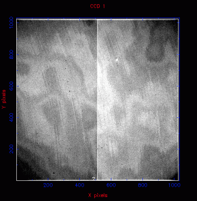
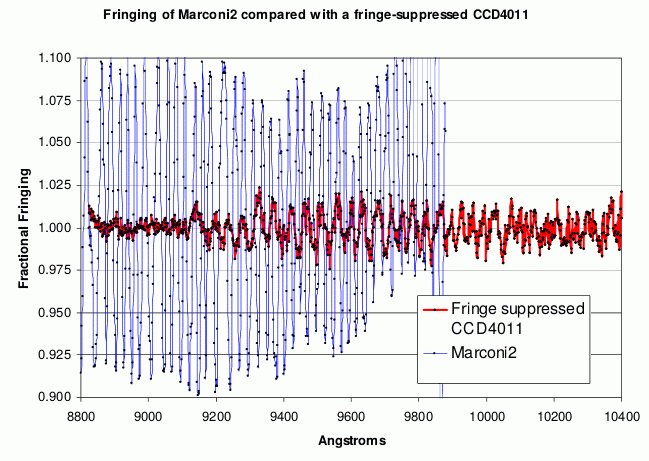
Back-thinned CCDs do have a number of disadvantages. Thinning can reduce the red response because red photons need more absorption length and if this is not there they will pass right through the silicon. Thinned CCDs are also mechanically fragile, prone to warping and expensive to manufacture compared to thick CCDs. Another problem is that the thin silicon layer produces interference fringing in the red part of the spectrum, as shown in figure 115. This is correctable to some extent at the data reduction stage, but fringing can limit the accuracy of measurements, particularly when doing spectroscopy.
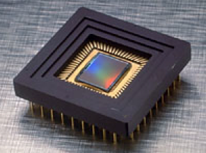
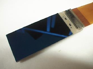
| figure 114: |
Left: photograph of a
thick front-side illuminated CCD, with the electrode structure on the
top. Right: photograph of
a thinned, back-side illuminated CCD, which appears almost black
thanks to the anti-reflection coating.
|
Fortunately, there is a way round the poor red-response of back-thinned CCDs, and that is by using thicker silicon (typically ~40 μm). Simply making the silicon thicker however, would mean that red photons would tend to generate charge below the depletion region. In this field-free region, the charge would then be able to diffuse in a random manner away from the point of generation before being attracted to the depletion region of a pixel for storage. The probability of being collected in the correct pixel is therefore reduced, effectively degrading the spatial resolution of the image. This problem can be alleviated by increasing the thickness of the depletion region, which is achieved by reducing the doping concentration of the silicon, i.e. using purer, higher-resistivity silicon. Such devices are known as deep-depletion CCDs. As well as significantly higher QE in the red, these devices exhibit much lower levels of fringing, due to the thicker silicon altering the condition for interference and also allowing more red light to be absorbed by the silicon rather than being reflected off the top and bottom surfaces and interfering. It is possible to obtain even lower levels of fringing in deep-depletion devices by altering the thicknesses of adjacent electrodes, a process sometimes referred to as anti-etaloning or fringe suppression, thereby further breaking the interference condition.
| figure 115: |
Left: an ULTRACAM z' CCD image showing fringing. Right:
fringe amplitude as a function of wavelength for a deep-depletion
CCD (blue) and a fringe-suppressed deep-depletion CCD (red).
|
Readout speed (For Advanced Readers)
CCDs are slow to read out due to the serial nature of the clocking and charge measurement processes. Typical dead times between CCD exposures are of order tens of seconds to minutes. Increasing the clocking and charge measurement speeds can decrease the dead time, but only at the expense of poor charge-transfer efficiency and readout noise, respectively. One way round this is to use a different CCD architecture, known as a frame-transfer CCD. Further details of frame-transfer CCDs can be found in the paper on the high-speed camera ULTRACAM by Dhillon et al. (2007).
Readout noise (For Advanced Readers)
There are a number of ways in which readout noise can be reduced in CCDs. One way is ensure that the CCD is manufactured using low-noise amplifiers at the outputs. A second way is to use a different CCD architecture, known as an electron-multiplying CCD (or EMCCD). Further details of EMCCDs can be found in the paper by Tulloch and Dhillon (2011).
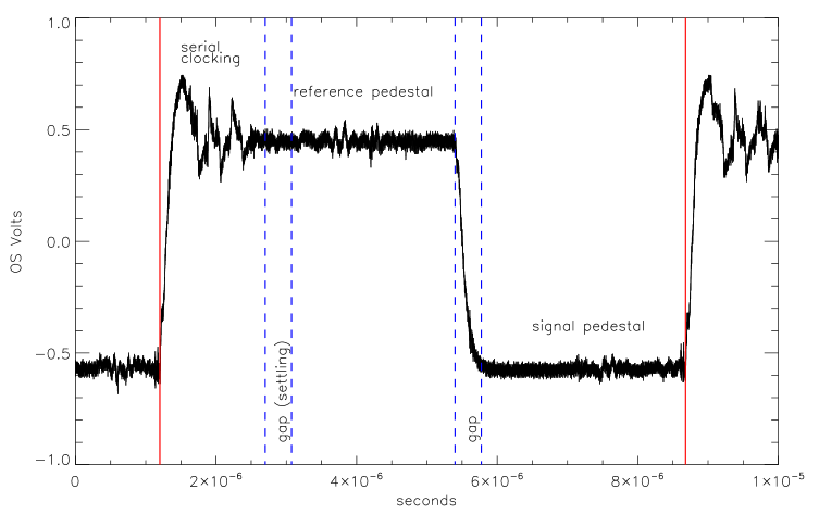
A third way of reducing CCD readout noise is to optimize the way in which the charge content of each pixel is measured. This measurement is performed by the video processor in the CCD controller. The video processor measures the size of the voltage step produced by the dumping of the charge in a pixel onto the output node of the CCD, as described earlier. Two measurements have to be made, a reference voltage before the charge is dumped (i.e. after the capacitor has been "reset"), and a signal voltage after the charge in each pixel has been dumped into it, as shown in figure 116. However, due to random thermal agitation of electrons in the reset electronics, there is uncertainty in the reset level, given by the reset noise = (kTC/e)0.5 e-, where k is Boltzmann's constant, e is the charge on the electron, T is the temperature of the capacitor and C is its capacitance. This noise is also sometimes referred to as kTC noise and is of order 100 e-. Fortunately, with suitable electronic design of the CCD output, the effect of reset noise can be eliminated as the (unknown) reference voltage is "frozen" once set, which means that taking the difference between the voltage measured after reset and after the pixel charge dump eliminates the reference voltage regardless of its value. This technique is known as correlated double sampling (or CDS), because two samples of the CCD output voltage are taken per pixel and the offset due to the reset noise in each sample is the same, i.e. it is correlated. Two common implementations of CDS are the dual slope integrator (or differential averager) and clamp and sample, which are described in more detail by Hegyi and Burrows (1980), Hopkinson and Lumb (1982), Tulloch (2013a) and Tulloch (2013b). The dual slope integrator takes two samples of equal duration, one before and one after the pixel dump. In clamp and sample, only a single sample after the pixel dump is taken (prior to this, the signal processing chain is clamped to ground for a brief period to establish a known reset level and then the clamp is open to let the signal go through the chain). The dual slope integrator is hence slower than clamp and sample, but results in better noise performance.
| figure 116: |
The change in voltage at the output of a CCD as the charge in a single
pixel is measured. The reference level is at 0.5 V and the signal
level is at -0.5 V. The difference between the two gives the charge in
the pixel. Note that this waveform represents a large signal that is
close to the full-well capacity of the pixel. Typical astronomical
images will have much smaller waveform amplitudes - the sensitivity of
a modern CCD is approximately 8 µV/e-. From
Tulloch
(2013a).
|
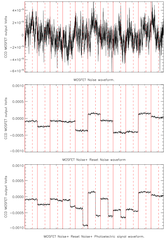
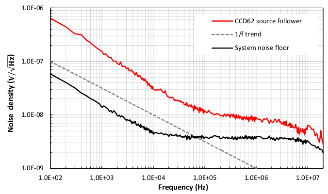
In practice, it isn't possible to measure the reference and signal voltages perfectly as both suffer from noise induced by the on-chip electronics, such as the MOSFETs in the output amplifier. The result is noise in the final output signal of the CCD, as shown in the top panel of figure 117. The power spectrum of this noise is shown in the left-hand panel of figure 118, where the x-axis is the frequency at which the pixels are read out by the CCD. At high frequencies, or fast pixel rates, the output signal from the CCD is dominated by white noise (also known as Johnson noise) from the amplifier, which is present at all frequencies and is constant with frequency. At lower frequencies, or slow pixel rates, the output of the CCD is dominated by 1/f noise (also known as flicker noise), where the noise increases with decreasing frequency. The effect of the high-frequency white noise can be minimised by integrating the reset level and the signal level, i.e. taking an average of each level using a dual-slope integrator instead of a single "snap-shot" measurement. Taking the difference of the average reset and signal levels using CDS also corrects for the lowest-frequency 1/f variations that occur on timescales longer than the signal-processing time for each pixel, as given by the separation of the vertical solid lines in figure 117. However, intermediate-frequency 1/f variations on timescales shorter than the pixel time are not corrected by the averaging, or by taking the difference between the reset and signal levels. Hence, as the integration time is increased, the readout noise decreases due to the reduction of the white noise component until a noise floor is reached of approximately 2 e-/pixel set by the 1/f noise, as shown in the right-hand panel of figure 118. Note that building a CCD controller that is capable of reaching the intrinsic noise floor of a modern CCD is extremely demanding.
| figure 117: |
Simulated output of a CCD
(in Volts) as a function of time, for 11 pixels. The solid, vertical
red lines show the pixel boundaries. The vertical, dashed red lines
show the charge dump event for each pixel. The top panel shows just
the noise from the output amplifier: two main noise components are
present - the short-timescale (white) noise and the longer timescale
flicker (1/f) noise. The power spectrum of these data are
shown in figure 118. The middle panel shows
the addition of the reset (or kTC) noise. The bottom panel
shows the addition of the signal. From
Tulloch
(2013a).
|
| figure 118: |
Left:
power
spectrum of the output of a CCD (red curve). 1/f noise is
dominant at lower frequencies, and the curve flattens off to white
noise at higher frequencies. The point at which it flattens, called
the corner frequency (or knee), lies at around 150 kHz for
this CCD, and is where the white noise is approximately equal to
the 1/f noise. Reading the CCD slower than the corner
frequency will not decrease the readout noise any further. Right: the
relationship between CCD readout noise and the pixel frequency. The
latter is proportional to the time taken to integrate the reset and
signal levels in the CDS. It can be seen that a noise floor is reached
around 20 kHz for this particular CCD, due to 1/f noise. It
can also be seen that the dual-slope integrator performs better than
the clamp and sample technique at all but the highest
frequencies. Both techniques gives better readout noise than predicted
by the CCD manufacturer (solid curve), most probably because they
include the effect of noise added by the CCD controller. From
Tulloch
(2013a).
|
Recent developments in CCD controller technology, in particular faster ADCs, now allow the use of digital CDS (DCDS). In this technique, rather than integrating the reset and signal levels using analogue electronics, a series of rapid "snap-shot" measurements of each level are made and digitised, as shown in figure 119. With multiple samples of each level now available, a range of averaging and weighting schemes can be adopted to maximise the signal-to-noise ratio of the CCD output. There have been claims of significantly reduced readout noise using DCDS (e.g. Cancelo et al. 2011), but Tulloch (2013a, 2013b, 2015) has shown that DCDS does not make all that much difference to the readout noise. According to Tulloch (priv. comm.), assuming that one has a well-designed analogue CCD controller with which to compare, the only advantages of DCDS are: 1. Cleaner/simpler CCD output electronics, e.g. no noisy switches, and; 2. Improved dynamic range due to the use of floating point arithmetic, effectively giving 1-2 more bits of ADC resolution - this means that quantization noise is not as important for high gains (e-/ADU). See also the papers on DCDS by Alessandri et al. (2015) and Alessandri et al. (2016), which support Tulloch's conclusions.
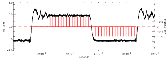
| figure 119: |
The change in voltage at the output of a CCD as the charge in a single
pixel is measured. The reference level is at 0.5 V and the signal
level is at -0.5 V. The red lines show the times that the waveform is
sampled for DCDS. In this scheme, the samples all have equal weights
but opposite signs (+1 in the first pulse group, -1 in the second
group), so this is the digital equivalent to the analogue dual-slope
integrator (differential averager). From
Tulloch
(2013a).
|