| output electronics |
|
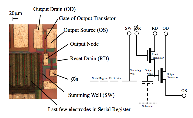
A detailed view of the output amplifier of a CCD is shown in figure 109. As each packet of electrons of total charge Q leaves the last pixel in the serial register, it is passed into a capacitor of capacitance C. This causes a small change in the voltage, V, across the capacitor, given by V = Q / C. This voltage change is first amplified and then measured. To measure the voltage, it is necessary define a reset level, i.e. the voltage across the capacitor in the absence of the charge contained in the CCD pixel. A technique known as correlated double sampling (CDS) is then used to measure the difference between the reset level voltage and the final voltage across the capacitor containing the charge packet. The faster the CDS is performed, the less accurate the measurement of the voltage. Finally, the voltage produced by each charge packet is digitized using an analogue-to-digital converter, producing the number of analogue-to-digital units (ADUs), or simply counts, in each pixel, which are then written to a computer disk.
| figure 109: |
Photomicrograph
of the output amplifier of a CCD and its circuit diagram.
|
There are a number of noise sources in the output electronics and the charge-measurement process that result in an uncertainty in the measurement of the charge contained in each pixel. This is known as readout noise, which can be reduced to a level of ~3 e- per pixel in a well-designed and well-optimized CCD.
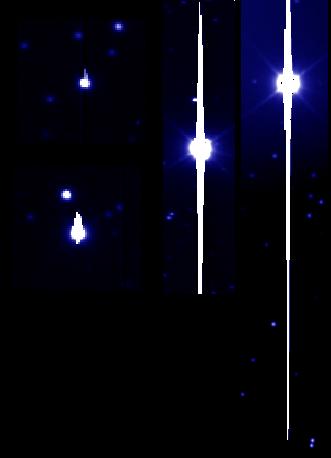
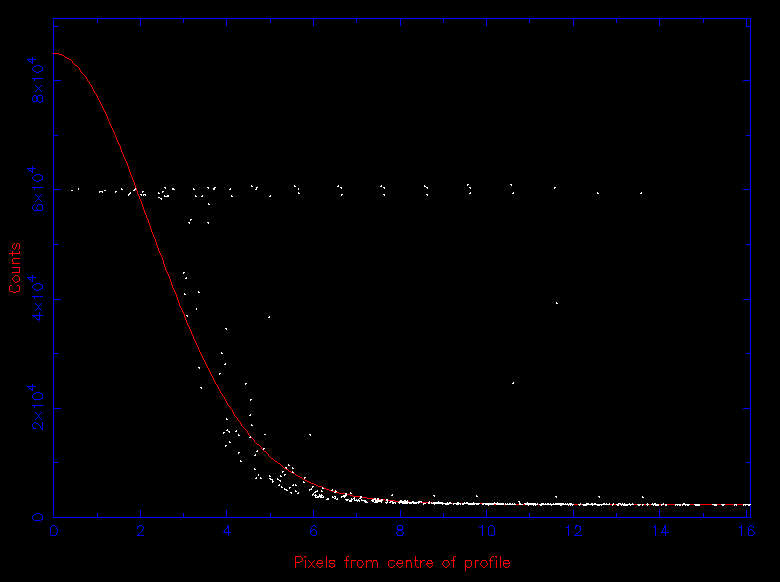
Each CCD pixel has a maximum charge carrying ability, known as the full-well capacity. Typically, the full-well capacity of a pixel is hundreds of thousands of electrons. If this is exceeded, no further electrons can be detected by that pixel and it is said to be saturated. The channel stops prevent any excess charge from spilling horizontally into adjacent pixels, so the electrons spill vertically into adjacent pixels, creating streaks in saturated images, known as blooming, as shown in figure 110. At the other end of the scale, the readout noise defines the lowest number of electrons that can be recorded. The ratio of the full-well capacity to the readout noise is known as the dynamic range of the CCD, and is typically of order 100,000:1.
| figure 110: |
Left: three CCD images showing the effects of saturation on a star. The level of saturation increases from left to right, evident as an increased level of blooming.
Right: the flat-topped point-spread-function of a saturated star.
|
Most high-quality CCDs have 16-bit analogue-to-digital converters (ADCs). This means that the ADC can divide a specified voltage into 216-1 = 65535 parts. For example, if the amplified voltage across the capacitor is 10 volts, voltage intervals as small as 152.6 μV can be measured, and each such interval would represent 1 count. Matching the amplified voltage to the resolution of the ADC is crucial. This is controlled by a parameter known as the gain, often given in units of e-/ADU. For the low signal levels typical in astronomy, it is important that the gain is set to a value such that the readout noise is optimally sampled. For example, if the readout noise of a CCD is 2 e-, and the gain is set to 4 e-/ADU, then it will be impossible to distinguish between pixels containing 1 or 2 units of readout noise, effectively increasing the readout noise. This so-called quantization noise is like a rounding error, but it can be rendered negligible by choosing an appropriate gain value: in the above example, a gain of approximately 1 e-/ADU should be used.
One consequence of using low gains to reduce quantization noise, however, is that the dynamic range of the CCD is defined not by the full-well capacity of a pixel but by the resolution of the ADC. For example, a gain of 1.5 e-/ADU would mean that a 16-bit ADC is capable of counting 1.5 x 65535 = 98302 e- before saturating. If the full-well capacity of the pixel is 200,000 e-, this means that the ADC would saturate well before the full-well capacity of the pixel is reached, i.e. the maximum number of electrons that can be counted is 98302, not 200,000. Another example is given in the example problems.
Note that the error due to quantization noise is given by the expression Nfwc / (2n . 120.5), where Nfwc is the effective full-well capacity of the pixel in electrons (i.e. the maximum number of electrons that can be counted by the ADC without saturating) and n is the number of bits in the ADC. For a well optimised CCD, Nfwc / 2n ≅ g, where g is the gain in e-/ADU, and hence the quantization noise is given by g / 120.5. Quantization noise must be added in quadrature with other CCD noise sources to give the total noise. For example, in a CCD with g = 1 e-/ADU and readout noise of 4 e-, the total noise becomes 4.01 e-, so quantization noise is unimportant. But in a CCD with g = 8 e-/ADU and readout noise of 4 e-, the total noise becomes 4.6 e-.