| the physics of semi-conductors |
|
One way of detecting light is to harness the photo-electric effect, where electrons are emitted from matter as a result of the absorption of a photon. To make a useful detector, however, some means of storing the electrons at the location where they were emitted, and then counting how many have been emitted in a given time, is required. The best way of doing this is to use a semi-conductor, so in this section we shall review the physics of this material and how it can be used to store and control the motion of electrons.
metals, semi-conductors and insulators
The energy levels available to bound electrons in an isolated atom are confined to certain discrete values. When isolated atoms are brought together to form a solid, they interact and their energy levels are split into a large number of closely spaced levels, creating a series of bands, as shown in figure 100.
| figure 100: |
Schematic showing the valence and conduction bands in a metal, semi-conductor
and insulator.
|
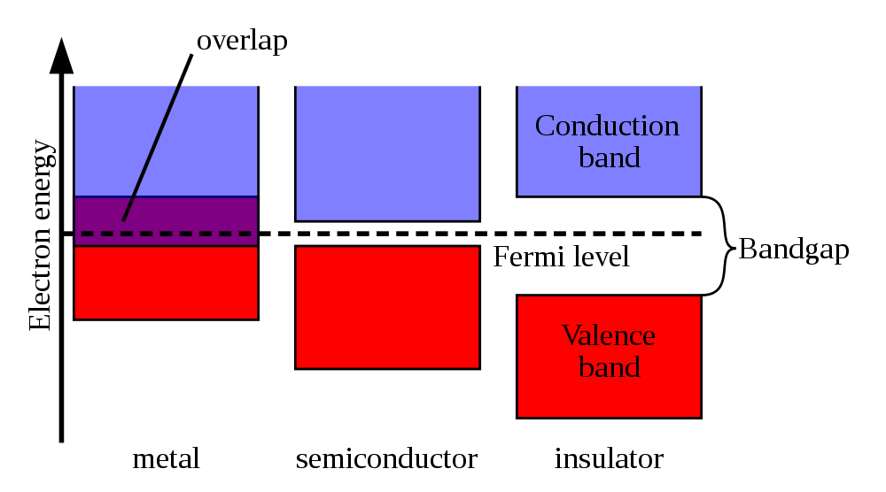
The highest energy levels interact the most and hence their bands are the widest. The highest energy band that is filled with electrons is known as the valence band. The band above this, composed of even higher energy, unoccupied levels, is called the conduction band. In an insulator, there is a wide gap between the valence and conduction bands, the band gap, which electrons are forbidden to occupy. The electrons in the completely filled valence band cannot move in response to an electric field because every nearby orbit in the valence band is occupied, and they do not have sufficient energy to move up into the conduction band. In a metal, the valence and conduction bands overlap, i.e. there is no band gap. In this case, the valence-band electrons are free to move throughout the solid in response to the force of an applied electric field, e.g. as produced when both ends of the metal are attached to a battery.
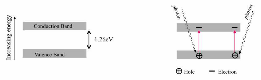
In a semi-conductor, the band gap is small. This means that it is sometimes possible for an electron to be promoted from the valence band to the conduction band by absorbing energy, either from the thermal motion of the atoms in the solid, or from an incoming photon, as shown in figure 101. Once an electron is in the conduction band, it can move and hence conduct electricity. The promoted electron leaves behind a hole in the valence band, and this too can conduct electricity, as it offers a place for neighbouring electrons to occupy. Since there are fewer charge carriers (electrons in the conduction band, holes in the valence band) in a semi-conductor than in a metal, semi-conductors are poorer conductors than metals, but better than insulators.
| figure 101: |
Schematic showing how a
photon of energy greater than 1.26 eV (the band gap of silicon) is able
to promote an electron to the conduction band, leaving behind a hole in
the valence band.
|
The semi-conductor of choice for CCDs is silicon, as it has a relatively large band gap, and hence is less likely to suffer from random elevation of electrons to the conduction band via thermal excitation, although this effect can be alleviated by cooling. Electrons that are elevated to the conduction band via the absorption of a photon are known as photo-electrons. The likelihood of absorbing a photon in silicon is a function of the photon energy, with red (low-energy) photons passing deeper into the silicon before being absorbed. A point comes when the reddest light does not have enough energy to overcome the band gap and promote a valence electron into the conduction band. For silicon, this occurs at a wavelength of approximately 1100 nm.
Unfortunately, once a photo-electron has been created in a silicon crystal, it is free to migrate through the crystalline structure, away from the point of origin, and recombine with a hole. Hence some means of separating the photo-electrons from the holes and storing them close to the point of origin is required. The best way of doing this is to use a p-n junction, as described below.
p-n junctions
The properties of a semi-conductor can be altered by deliberately adding small amounts of impurities, a process known as doping. Doped silicon in which the impurity has more valence electrons than undoped silicon will donate these negatively-charged electrons to the conduction band and is hence known as n type. Conversely, doped silicon with a deficit of valence electrons compared to undoped silicon will leave a positively charged hole in the valence band ready to accept any electrons, and is hence known as p type. If an n-type and p-type semi-conductor are brought together, a p-n junction is formed. Electrons from the n region will diffuse to the p region to fill up some of the holes in the valence band, thus making the p region more negative than it was. Similarly, the diffusion of holes from the p region to the n region will make the n region more positively charged than it was. Therefore, a narrow zone, the depletion region or space charge region, either side of the junction will form where the majority charge carriers are depleted relative to their concentrations well away from the junction, as shown in figure 102. Eventually, a potential barrier is created by the build up of electrons and holes on the p and n sides, respectively, repelling further diffusion.
| figure 102: |
Schematic
showing a p-n junction. The concentration of electrons and holes are
shown by the blue and red lines, respectively. The grey regions are
neutral, the red zone is positively charged and the blue zone is
negatively charged. The directions of the electric field, the
electrostatic force on the electrons and holes, and the direction in
which the diffusion tends to move electrons and holes, are shown at
the bottom.
|
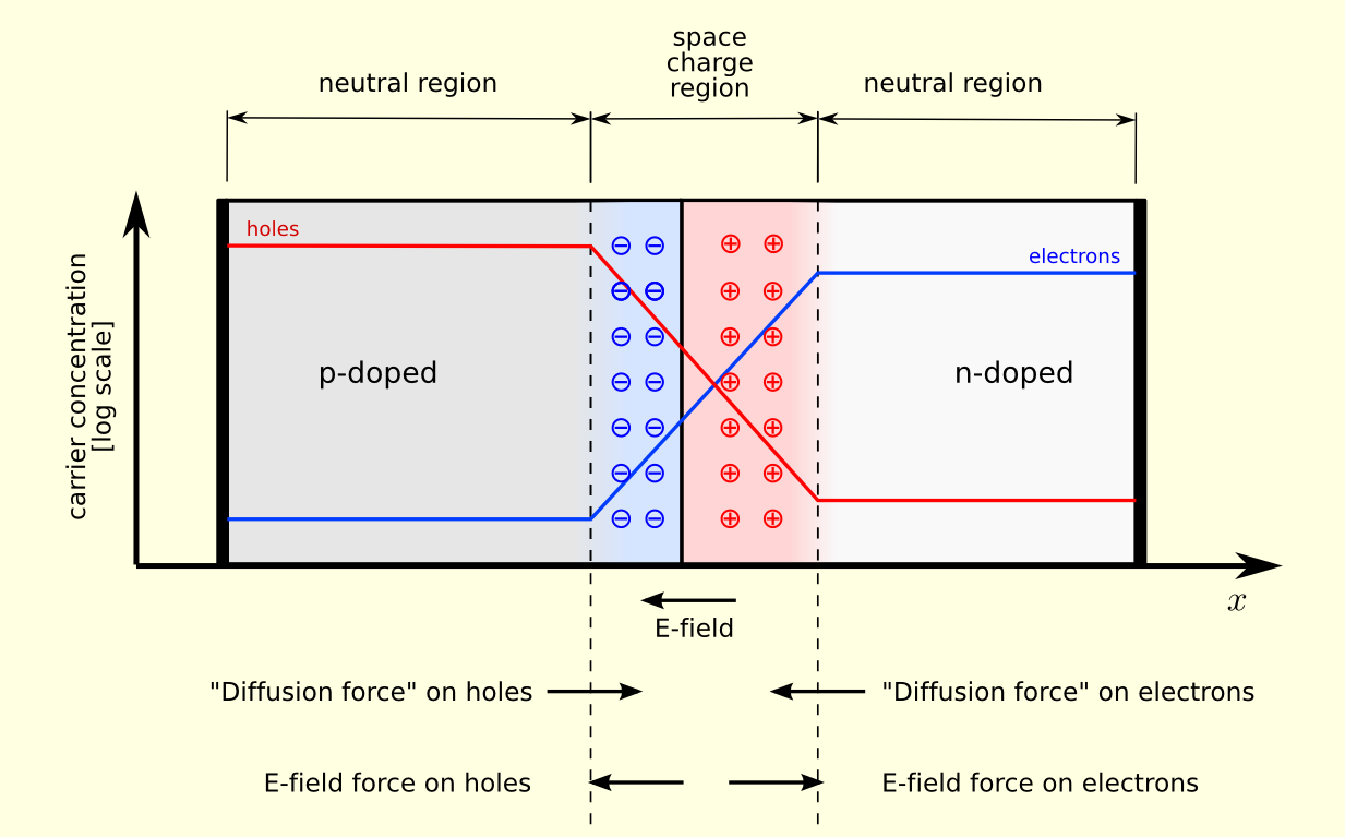
The concentration of holes buried in the n-type region will have a more positive electrical potential than elsewhere in the crystal, whereas the surplus of electrons in the p-type region will make it more negative. This means that any electron-hole pairs created near the junction by incoming photons will be swept apart and the electrons will be stored in the region of greatest positive potential in the n-type layer, which therefore acts as a charge storage capacitor.
It possible to control the height of the potential barrier and the width of the depletion region by applying a voltage across the junction, which in turn controls the capacity of the p-n junction to store charge. If a positive voltage is applied to the p side of the p-n junction, it will tend to attract more electrons across the junction and decrease the potential barrier (the forward bias condition). More usefully for CCDs, a positive voltage applied to the n side would increase the potential barrier and the width of the depletion region (the reverse bias condition).